게시판
최근논문
-
[Editor's Pick] Current Optics and Photonics Vol. 8 no. 2 (2024 April)
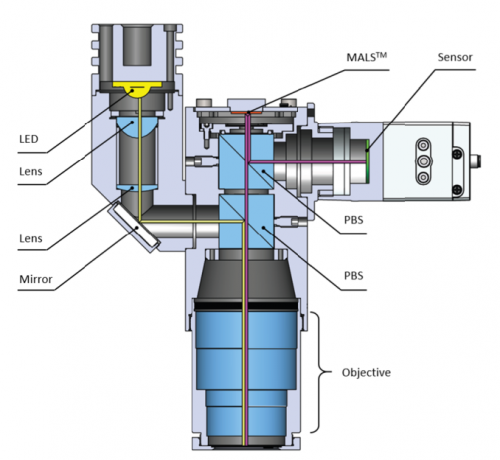
Quantifying Aberrations on Object Plane Using Zernike Polynomials
Yohan Kim1 *, Theo Nam Sohn2, Cheong Soo Seo1, and Jin Young Sohn1
Current Optics and Photonics Vol. 8 No. 2 (2024 April), pp. 151-155
DOI: https://doi.org/10.3807/COPP.2024.8.2.151
Fig. 1 Optical layout of 1.5× magnification WiseScope. LED, light-emitting diode; PBS, polarizing beam splitter.
Keywords: Focus measure, Optical aberration, Wavefront error, Zernike polynomials
OCIS codes: (010.7350) Wave-front sensing; (080.1010) Aberrations (global); (100.2550) Focalplane-array image processors; (110.0110) Imaging systems; (120.4640) Optical instruments
Abstract
Optical systems often suffer from optical aberrations caused by imperfect hardware, which places significant constraints on their utility and performance. To reduce these undesirable effects, a comprehensive understanding of the aberrations inherent to optical systems is needed. This article presents an effective method for aberration detection using Zernike polynomials. The process involves scanning the object plane to identify the optimal focus and subsequently fitting the acquired focus data to Zernike polynomials. This fitting procedure facilitates the analysis of various aberrations in the optical system.
-
[하이라이트 논문] 한국광학회지 Vol. 35 No.2 (2024 April)
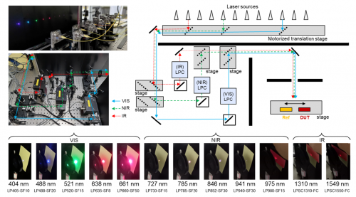
12개 다이오드 레이저를 활용하는 레이저 복사출력계 교정시스템 개발
Development of Laser Power Meter Calibration System with 12-diode Laser Sources
이강희ㆍ유재근ㆍ배인호ㆍ박성종ㆍ이동훈1†
한국광학회지 Vol. 35 No.2 (2024 April) pp. 61-70
DOI: https://doi.org/10.3807/KJOP.2024.35.2.061
Fig. 1 Schematics and photographs of the laser power calibration system. Commercially available fiber-coupled laser diodes (Thorlabs,) are used, and the model names of the lasers are listed below their wavelengths. Three laser power controllers (LPC; BEOC) are additionally used for laser power stabilization. The system is designed to automatically select the laser for the calibration process using multiple motorized translation stages. In the schematics, DUT denotes device under test, while Ref denotes reference for the calibration.
Keywords: 검출기 기반 복사 측정, 레이저 복사출력계 교정, 적분구
OCIS codes: (120.3150) Integrating spheres; (120.5630) Radiometry; (140.2020) Diode lasers; (230.5170) Photodiodes
초록
400 nm부터 1,600 nm까지의 파장 영역에서 단일 모드 광섬유에 결합된 12개의 다이오드 레이저 광원를 기반으로 하는 레이저 복사출력계 교정시스템을 소개한다. 본 시스템은 복사출력 측정위치에서 레이저 출력요동을 최소화하였고 모든 광원에 대해 비슷한 빔크기를 갖는다. 또한 감응도의 비균일도 및 비선형성을 최소화하기 위해 적분구 기준기를 사용하였다. 이 교정시스템의 최소 측정불확도는 대부분의 레이저 파장에서 1.1% (k = 2)로 추정된다.
Abstract
We demonstrate a laser power meter calibration system based on 12-diode laser sources coupled to single-mode fibres in a wavelength range from 400 to 1,600 nm. In our system, three laser power controllers ensure that the output power uncertainty of all laser sources is less than 0.1% (k = 2). In addition, all laser beams are adjusted to have similar beam sizes of approximately 2 mm (1/e 2 -width) at the measurement position to minimise unmeasured laser power on a detector. As a reference detector, we use an integrating sphere combined with silicon and indium gallium arsenide photodiodes to minimise the non-uniformity and non-linearity of responsivity. The minimum uncertainty of the calibration system is estimated to be 1.1% (k = 2) for most laser wavelengths.
-
[Editor's Pick] Current Optics and Photonics Vol. 8 no. 1 (2024 February)
SLODAR System Development for Vertical Atmospheric Disturbance Profiling at Geochang Observatory
Ji Yong Joo1, Hyeon Seung Ha1, Jun Ho Lee1,2 *, Do Hwan Jung1,3, Young Soo Kim1,3, and Timothy Butterley4
Current Optics and Photonics Vol. 8 No. 1 (2024 February) pp. 30-37
DOI: https://doi.org/10.3807/COPP.2024.8.1.30
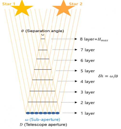
Fig. 1 Schematic diagram illustrating the crossed-beam method. This specific diagram depicts the construction of 8 layers of vertical profiling with 8 sub-aperture wavefront sensing [13].
Keywords: Adaptive optics, Atmospheric turbulence, Fried parameter, Refractive index structure function (C2n), SLODAR
OCIS codes: (010.1330) Atmospheric turbulence; (120.4640) Optical instruments; (220.1080) Active or adaptive optics; (350.1260) Astronomical optics
Abstract
Implemented at the Geochang Observatory in South Korea, our slope detection and ranging (SLODAR) system features a 508 mm Cassegrain telescope (f /7.8), incorporating two Shack-Hartmann wave-front sensors (WFS) for precise measurements of atmospheric phase distortions, particularly from nearby binary or double stars, utilizing an 8 × 8 grid of sampling points. With an ability to reconstruct eight-layer vertical atmospheric profiles, the system quantifies the refractive index structure function (C2n) through the crossed-beam method. Adaptable in vertical profiling altitude, ranging from a few hundred meters to several kilometers, contingent on the separation angle of binary stars, the system operates in both wide (2.5 to 12.5 arcminute separation angle) and narrow modes (11 to 15 arcsecond separation angle), covering altitudes from 122.3 to 611.5 meters and 6.1 to 8.3 kilometers, respectively. Initial measurements at the Geochang Observatory indicated C values up to 181.7 meters with a Fried parameter (r0) of 8.4 centimeters in wide mode and up to 7.8 kilometers with an r0 of 8.0 centimeters in narrow mode, suggesting similar seeing conditions to the Bohyun Observatory and aligning with a comparable 2014–2015 seeing profiling campaign in South Korea.
-
-
[Editor's Pick] Current Optics and Photonics Vol. 7 no. 6 (2023 December)
Femtosecond Mid-IR Cr:ZnS Laser with Transmitting Graphene-ZnSe Saturable Absorber
Won Bae Cho1 *, Ji Eun Bae2, Seong Cheol Lee2, No Soung Myoung3, and Fabian Rotermund2
Current Optics and Photonics Vol. 7 No. 6 (2023 December) pp. 738-744
DOI: https://doi.org/10.3807/COPP.2023.7.6.738
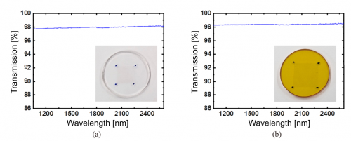
Fig. 1 Optical transmission of high-quality monolayer graphene saturable absorber (G-SA) and photos of the G-SAs developed on CaF2 and ZnSe substrate (inset). (a) Graphene transferred onto CaF2 substrate. (b) Graphene transferred onto ZnSe substrate.
Keywords: Cr:ZnS, Graphene-ZnSe, Mid-infrared laser, Passive mode-locking, Saturable absorber
OCIS codes: (140.4050) Mode-locked lasers; (140.7090) Ultrafast lasers; (160.4236) Nanomaterials; (160.4330) Nonlinear optical materials
Abstract
Graphene-based saturable absorbers (SAs) are widely used as laser mode-lockers at various laser oscillators. In particular, transmission-type graphene-SAs with ultrabroad spectral coverage are typically manufactured on transparent substrates with low nonlinearity to minimize the effects on the oscillators. Here, we developed two types of transmitting graphene SAs based on CaF2 and ZnSe. Using the graphene-SA based on CaF2, a passively mode-locked mid-infrared Cr:ZnS laser delivers relatively long 540 fs pulses with a maximum output power of up to 760 mW. In the negative net cavity dispersion regime, the pulse width was not reduced further by inhomogeneous group delay dispersion (GDD) compensation. In the same laser cavity, we replaced only the graphene-SA based on CaF2 with the SA based on ZnSe. Due to the additional self-phase modulation effect induced by the ZnSe substrate with high nonlinearity, the stably mode-locked Cr:ZnS laser produced Fourier transform-limited ~130 fs near 2,340 nm. In the stable single-pulse operation regime, average output powers up to 635 mW at 234 MHz repetition rates were achieved. To our knowledge, this is the first attempt to achieve shorter pulse widths from a polycrystalline Cr:ZnS laser by utilizing the graphene deposited on the substrate with high nonlinearity.
-
[하이라이트 논문] 한국광학회지 Vol. 34 No.6 (2023 December)
반사형 Focal Reducer를 가지는 높은 개구수의 대물렌즈 설계
Optical Design of a High-numerical-aperture Objective with a Reflective Focal Reducer
이종웅1†
한국광학회지 Vol. 34 No.6 (2023 December) pp. 248-260
DOI: https://doi.org/10.3807/KJOP.2023.34.6.248
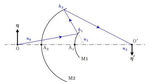
Fig. 1 Optical layout of a two-spherical mirror system.
Keywords: 아나스티그마트, 고해상 대물렌즈, 반사형 포컬 리듀서, 2구면경계
OCIS codes: (080.4035) Mirror system design; (110.0180) Microscopy; (220.1000) Aberration compensation; (220.3620) Lens system design
초록
낮은 NA의 굴절형 대물렌즈와 반사형 focal reducer로 구성된 NA 0.5의 굴절-반사 대물렌즈를 설계하였다. 굴절형 대물렌즈로는 NA 0.25 인 Lister 대물렌즈가 사용되고, 반사형 focal reducer는 구면수차, 코마, 비점수차가 보정된 2구면경계가 사용되었다. 설계된 굴절-반사 대물렌즈는 높은 NA를 가졌음에도 18 mm의 긴 작동거리와 NA 0.25의 Lister 대물렌즈보다 개선된 결상성능을 가지고 있다.
Abstract
A 0.5-NA refractive-reflective objective, composed of a low-NA refractive and a reflective focal reducer, is designed. A 0.25-NA Lister objective is used for the refractive. A two-spherical-mirror system, corrected for spherical aberration, coma, and astigmatism is used for the reflective focal reducer. In spite of high NA, the refractive-reflective objective has an 18-mm working distance and improved imaging performance, compared to the 0.25-NA Lister objective.
-
[Editor's Pick] Current Optics and Photonics Vol. 7 no. 5 (2023 October)
Volume-sharing Multi-aperture Imaging (VMAI): A Potential Approach for Volume Reduction for Space-borne Imagers
Jun Ho Lee1,2 *, Seok Gi Han1, Do Hee Kim1, Seokyoung Ju1, Tae Kyung Lee3, Chang Hoon Song3, Myoungjoo Kang3, Seonghui Kim4, and Seohyun Seong4
Current Optics and Photonics Vol. 7 No. 5 (2023 October) pp. 545-556
DOI: https://doi.org/10.3807/COPP.2023.7.5.545
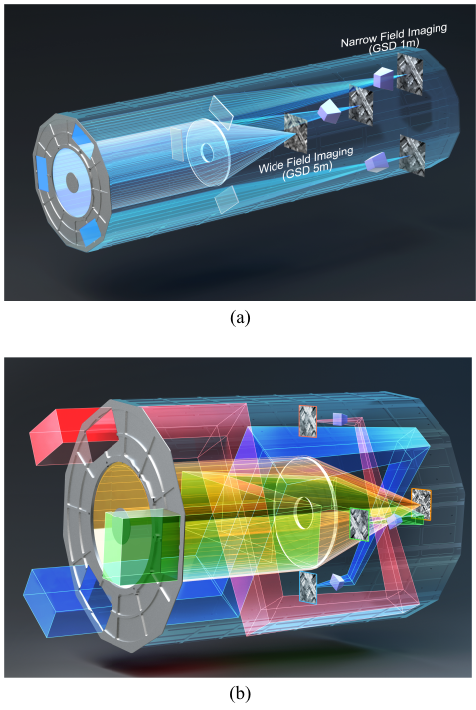
Fig. 2 Illustration of volume-sharing multi-aperture imaging (VMAI) with one wide-field and three narrow-field cameras: (a) Unfolded and (b) compactly folded.
Keywords: Deep-learning, Earth observation, Image fusion, Volume-sharing multi-aperture imaging
OCIS codes: (110.3010) Image reconstruction techniques; (120.3620) Lens system design;(120.4640) Optical instruments; (220.4830) Systems design; (220.4991) Passive remote sensing
Abstract
This paper introduces volume-sharing multi-aperture imaging (VMAI), a potential approach proposed for volume reduction in space-borne imagers, with the aim of achieving high-resolution ground spatial imagery using deep learning methods, with reduced volume compared to conventional approaches. As an intermediate step in the VMAI payload development, we present a phase-1 design targeting a 1-meter ground sampling distance (GSD) at 500 km altitude. Although its optical imaging capability does not surpass conventional approaches, it remains attractive for specific applications on small satellite platforms, particularly surveillance missions. The design integrates one wide-field and three narrowfield cameras with volume sharing and no optical interference. Capturing independent images from the four cameras, the payload emulates a large circular aperture to address diffraction and synthesizes highresolution images using deep learning. Computational simulations validated the VMAI approach, while addressing challenges like lower signal-to-noise (SNR) values resulting from aperture segmentation. Future work will focus on further reducing the reduction ratio and refining SNR management.
-
-
[Editor's Pick] Current Optics and Photonics Vol. 7 no. 4 (2023 August)
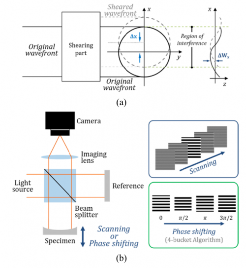
Shearing Interferometry: Recent Research Trends and Applications
Ki-Nam Joo* and Hyo Mi Park
Current Optics and Photonics Vol. 7 No. 4 (2023 August) pp. 325-336
DOI: https://doi.org/10.3807/COPP.2023.7.4.325
Fig. 1 Optical layout. (a) Shearing interferometry, and (b) typical interferometry.
Keywords: Azimuthal shearing interferometer, Lateral shearing interferometer, Radial shearing interferometer, Shearing interferometer, Wavefront reconstruction
OCIS codes: (120.3180) Interferometry; (120.3930) Metrological instrumentation; (120.6650) Surface measurements, figure
Abstract
We review recent research related to shearing interferometry, reported over the last two decades. Shearing interferometry is categorized as azimuthal, radial, or lateral shearing interferometers by its fundamental principle to generate interference. In this review the research trends for each technique are provided, with a summary of experimental results containing theoretical background, the optical configuration, analysis, and perspective on its application fields.
-
[하이라이트 논문] 한국광학회지 Vol. 34 No.4 (2023 August)
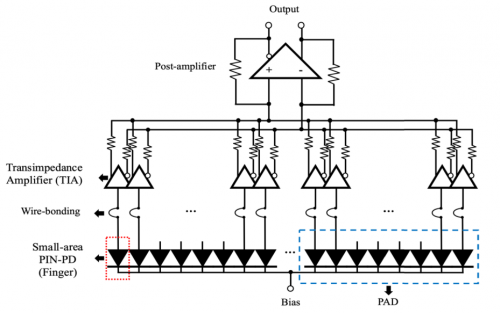
고성능 광각 3차원 스캐닝 라이다를 위한 스터드 기술 기반의 대면적 고속 단일 광 검출기
Large-area High-speed Single Photodetector Based on the Static Unitary Detector Technique for High-performance Wide-field-of-view 3D Scanning LiDAR
한문현ㆍ민봉기†
한국광학회지 Vol. 34 No.4 (2023 August) pp. 139-150
DOI: https://doi.org/10.3807/KJOP.2023.34.4.139
Fig. 1 Schematic of the large-area high-speed photodetector based on the static unitary detector (STUD) technique.
Keywords: 대면적, 라이다, 고속, 광 검출기, 스터드
OCIS codes: (040.5160) Photodetectors; (200.4560) Optical data processing; (280.3640) Lidar; (280.4788) Optical sensing and sensors
초록
다양한 구조의 라이다(light detection and ranging, LiDAR)가 존재함에도 불구하고 넓은 화각을 유지하면서 장거리 측정과 수직, 수평 방향 모두에서 높은 해상도를 만족하는 LiDAR를 구현하는 것은 매우 어렵다. 스캐닝 구조는 장거리 탐지 및 수직, 수평 방향에 대한 높은 해상도를 만족하는 고성능 LiDAR를 구현하는 데 유리하지만, 넓은 화각을 확보하기 위해서는 검출 속도에 불리한 대면적 광 검출기(photodetector, PD) 가 필수적이다. 따라서 이러한 문제점을 해결하기 위해 다수의 소면적 PD를 고속의 단일 대면적 PD로 작동할 수 있는 static unitary detector (STUD) 기술 기반의 PD를 제안하였다. 본 논문에서 제안하는 InP/InGaAs STUD PIN-PD는 1,256 μm × 19 μm의 단위 면적을 가지는 32 개 소면적 PD를 활용하여 1,256 μm × 949 μm 이내에서 다양한 형태로 설계 및 제작하였다. 이후 다양한 형태로 제작된 STUD PD의 특성과 감도는 물론 이를 활용한 LiDAR 수신 보드의 잡음 및 신호 특성에 대해 측정 및 분석하였다. 마지막으로 STUD PD가 적용된 LiDAR 수신 보드를 1.5-μm master oscillator power amplifier 레이저를 광원으로 활용하는 3차원 스캐닝 LiDAR 시제품에 적용하였고, 이를 통해 대각 32.6도의 광각에서 50 m 이상의 장거리 물체를 정밀하게 탐지하면서 320 px × 240 px의 고해상도 3차원 영상을 동시에 확보하였다.
Abstract
Despite various light detection and ranging (LiDAR) architectures, it is very difficult to achieve long-range detection and high resolution in both vertical and horizontal directions with a wide field of view (FOV). The scanning architecture is advantageous for high-performance LiDAR that can attain long-range detection and high resolution for vertical and horizontal directions. However, a large-area photodetector (PD), which is disadvantageous for detection speed, is essentially required to secure the wide FOV. Thus we propose a PD based on the static unitary detector (STUD) technique that can operate multiple small-area PDs as a single large-area PD at a high speed. The InP/InGaAs STUD PIN-PD proposed in this paper is fabricated in various types, ranging from 1,256 μm × 949 μm using 32 small-area PDs of 1,256 μm × 19 μm. In addition, we measure and analyze the noise and signal characteristics of the LiDAR receiving board, as well as the performance and sensitivity of various types of STUD PDs. Finally, the LiDAR receiving board utilizing the STUD PD is applied to a 3D scanning LiDAR prototype that uses a 1.5-μm master oscillator power amplifier laser. This LiDAR precisely detects long-range objects over 50 m away, and acquires high-resolution 3D images of 320 pixels × 240 pixels with a diagonal FOV of 32.6 degrees simultaneously.